ULTRA-PURE SILICON
Development of High-purity Silicon Mirrors for the Einstein Telescope
The Einstein Telescope (ET) will be a third-generation detector with a tenfold increase in sensitivity for gravitational waves that will expand the observing window for previously hidden cosmic events. ET will have the potential to discover new, so far unknown sources of gravitational waves. To achieve this extremely high sensitivity, the interferometer’s mirrors will be made of silicon crystals. Crystalline silicon offers excellent material properties for detection at cryogenic temperatures, where the interferometer will operate to minimise thermal noise.
High-purity silicon mirrors
The mirrors of the interferometer will be made of ultra-pure and highly perfect crystalline silicon to ensure that the interference patterns are not distorted by impurities or structural defects. Impurities and crystal defects such as dislocations would lead to scattering and absorption of the laser light, which would also increase the heat generation in the mirrors. This would significantly reduce the sensitivity of ET.
An industrially established method of producing dislocation-free, large diameter silicon single crystals is the Floating Zone (FZ) process. In this crucible-free growth method, the non-contact inductively heated melt is not contaminated by any other material. As a result, ultra-high crystal purity can be achieved, virtually limited only by the purity of the raw material. FZ silicon with a high specific electrical resistance of Ω > 10 kΩ cm has been measured to have the lowest absorption – α ≈4.3 ppm/cm compared to silicon from other manufacturing processes.
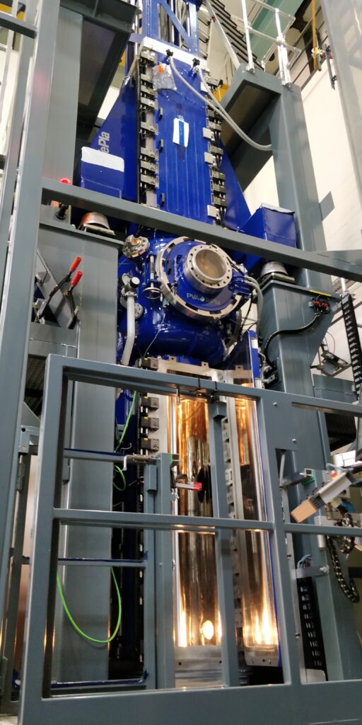
At the Leibniz-Institut für Kristallzüchtung in Berlin (IKZ), a new furnace for the FZ growth of large silicon crystals was put into operation in 2021. The new PVA-FZ30-M furnace has been used to successfully grow high-purity silicon crystals with a resistivity of more than 10 kΩ-cm and a diameter of 150 mm. These crystals will be tested in the experimental facility for laser interferometry at the ET Pathfinder research laboratory in Maastricht.
However, larger silicon crystals with a diameter of at least 450 mm are needed for the mirrors of the future Einstein telescope. It is not currently possible to grow crystals of this diameter using the Floating Zone (FZ) method. Other silicon crystal growth methods, such as the Czochralski or Quasi-Mono methods, have already produced crystals with the required diameter. But due to the use of quartz crucibles and graphite heaters in these methods, impurities such as oxygen, carbon and transition metals are introduced into the crystal, resulting in absorption levels that are at least an order of magnitude higher. There is currently no silicon crystal manufacturing process that combines the mirror diameter required for the Einstein telescope with ultra-high purity.
CONTRIBUTION TO SOCIETY: Applications in photovoltaics, microelectronics and power electronics
Crystalline silicon is the dominant semiconductor material for applications in photovoltaics, microelectronics and power electronics.
For power electronics in particular, ultra-high purity and perfection of these crystals are required. These crystal properties have a significant impact on the performance, reliability, lifetime, efficiency and energy consumption of power electronic devices. Ultra-high purity is often required for power semiconductors, which require a specific electrical resistance of the silicon substrate greater than 10 kΩ cm. Typical components for these applications include diodes and transistors such as MOSFETs (metal oxide semiconductor field effect transistors) and IGBTs (insulated gate bipolar transistors). High-voltage transistors, such as high-voltage IGBTs for voltages from 3.3 kV to 6.5 kV, are used in high-voltage direct current (HVDC/HVAC) transmission, power converters for solar and wind energy systems, electric trains and other heavy electric vehicles.
The low-cost availability of these components is critical to driving the green energy transition. The cost of power semiconductors is determined by several factors, including manufacturing technology, chip integration level and wafer size, all of which play a significant role.
There is a continuing demand for larger diameter silicon crystals as larger wafers allow more efficient utilisation of chip production facilities. By using larger wafers, more chips can be produced simultaneously, resulting in higher production capacity and improved efficiency of expensive production lines.
Currently, power semiconductors are mainly manufactured on 6-inch and 8-inch wafers. The industry has been slowly migrating from 8-inch to 12-inch wafers for years. The transition from 8-inch to 12-inch will increase production capacity per wafer by a factor of 2.25. Since there is no high-purity silicon crystal growth process such as the FZ process available for crystals larger than 8 inches in diameter, crystals for 12-inch wafers are grown using the Czochralski method.
To reduce the impurities introduced during Czochralski growth by the use of a crucible, magnetic fields are applied to influence the melt flow in a process called Magnetic Czochralski. Although this reduces impurities in the crystal, the concentrations of typical impurities such as oxygen and carbon remain an order of magnitude higher than in FZ crystals.
The growth of silicon crystals with a diameter of 18 inches – the size required for the Einstein telescope – using the Czochralski method has already been demonstrated. However, a 450mm wafer process has not yet been established in production. Advancing growth technologies for large, ultra-high-purity crystals, such as those required for the Einstein telescope mirrors, could be a game-changer for the semiconductor industry.